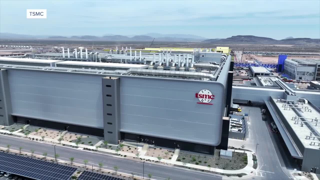


In the heart of the Arizona desert, some of the country's most advanced semiconductor chips are being manufactured at Taiwan Semiconductor Manufacturing Company's (TSMC) facility.
"Semiconductors are basically everything that's in your phone, in your computers. It's the brains of everything that has a power switch and anything that needs to compute," said TSMC Arizona's President, Rose Castanares.
Creating these tiny technological marvels is an incredibly complex process.
"Making a wafer is the most complicated manufacturing process in the world. I can't imagine anything else more difficult than this," said engineer Konstantinos Ninios.
The manufacturing requires up to 4,000 precise steps, and there's no room for error.
Step inside the Arizona TSMC facility with ABC15's Ben Brown and see part one of an exclusive three-part series, in the player below.
"You're done. You have to start from the beginning. This wafer cannot be used anymore," said Ninios.
What makes TSMC different from other semiconductor companies is its business model.
They don't design the chips, they build them customized for clients.
"That goes back to our pure-play foundry model. We have very in-depth discussions about how they want their chips to perform, if they want to be able to have different types of transistors, [and] if they want different types of metal layers. But in the end, it's their design and we manufacture for them," said Castanares.
The manufacturing happens inside a clean room — a tightly controlled environment where chips are created, tested, and perfected.
Workers like Sterling Wilson, an EBO [Exposure, Bit, Optical] mask technician, ensure quality control throughout the process.
"What I'm doing is EUV... Basically, an electric ultraviolet beam (EBL)... and I'm looking through this scope... at all these different things. Again, trying to make sure that exactly how we have our pattern is how they have their map," said Sterling.
TSMC's first fabrication facility (fab) is already operational in Phoenix, producing four-nanometer chips. But the company has much bigger plans.
Earlier this year, TSMC announced another $100 billion investment to ultimately build six fabs, a research and development center, and two advanced packaging facilities in Arizona.
When asked about the timeline for these expansions, Castanares told ABC15, "So 'Fab Two', we will be starting to move in equipment soon. For 'Fab Three', you can see that the building excavation has started, and we will be, hopefully, moving that construction as quickly as possible."
The company aims to have Fab Two operational by 2028 and Fab Three by the end of the decade, with them showing us some of the first looks at the Fab Three construction site.
"I think that it's going to take us a little bit of time to be able to get all of the permits and all of the construction crews that we need. But there's a huge demand, almost insatiable demand, for AI and high-performance computing, and so we'll be doing everything we can to make that a reality as soon as possible," Castanares said.
Watch part two of a three-part series as ABC15 takes an inside look at TSMC, in the player below:
As TSMC continues to expand its footprint in Arizona, the company is facing both growing pains and promising progress.
The company currently employs about 3,000 people in Arizona — one of the first was Jeff Patz, who trained at the company headquarters in Taiwan for over a year.
"There was a huge batch of us that all went there together, so kind of experience that new to the semiconductor industry, new to Taiwan altogether was pretty exciting," Patz said, who is currently an engineer at TSMC Arizona.
Currently, there are several hundred employees who are from Taiwan who were sent to install complex tech and train local hires to meet global standards.
“As that training and that know-how continues to build here in Arizona with our local hires, and it will take a little while, a couple of years, to get you know, really understanding how to, you know, troubleshoot and what to do when things go wrong,” Castanares said. "Then those folks from Taiwan, you know, can go back to their home fabs.”
But cultural differences have led to some growing pains, including several lawsuits alleging a toxic work culture.
"I would say, it’s almost like we go to Taiwan to train and we're bringing that culture here to the U.S. and the exciting part is like it's almost like when you bake a cake at high altitude or low altitude, you're still baking the same cake, but you have to make some fine tune adjustments.”)
Castanares acknowledged there will always be people with differences of opinion, but said the company is working to bridge the divide.
“If you have two people, you will always have differences of opinion. We have lots of different training programs so that people can understand the different types of cultures and different types of ways of communicating, different types of leadership,” Castanares told ABC15. “And it's a learning process. You know, we're not the first company to come and build a brand new, large plant, and it always takes a little bit of time."
Josie Cheng, an equipment engineer who started her career in Taiwan before transferring to TSMC Arizona, said there were cultural challenges at the beginning, but she feels that is no longer the case.
"The cultural thing is in the work, you know, Taiwanese culture, in the beginning, we try to crush each other,” Josie said. “We have some cultural [clash] in the beginning, and I think I'm used to it right now. I think we got the balance, and it's not the challenge anymore.”
As Fabs 2 and 3 near completion, thousands more engineers and technicians will be needed. TSMC is looking ahead, partnering with universities, and creating apprenticeship programs to create a pipeline to fill future demand.
Watch part three of a three-part series as ABC15 takes a look at TSMC's sustainability efforts, in the player below:
In addition to building more fabs, TSMC is looking at ways to be more sustainable in the future. Currently, TSMC recycles about 65% of the water it uses, but the goal is to build an industrial reclaimed water plan that would increase that number to 90% by 2028.
"Our long-term goal is to be 90 percent or better with our near-zero liquid discharge plant,” Greg Jackson, director of facilities at TSMC, told ABC15.
In addition, TSMC has installed solar panels to help reduce its energy use and scrubber exhaust stacks to keep pollutants out of the air.
“In the process we use chemicals, we have to capture those chemicals so it's safe and we can't just reject the air into the atmosphere,” Jackson said. "We run it through what we call water scrubbers that pull the air pollutants out of the air stream into the water, where we then recycle that water like we talked about earlier and the air coming out of the stacks is clean.”
TSMC still has a long way to go until it reaches its ultimate goal of six fabs, a research and development center, as well as advanced packaging facilities, but the idea is to have everything connected with sustainability at the forefront.
This story was reported by a journalist and has been converted to this platform with the assistance of AI. Our editorial team verifies all reporting on all platforms for fairness and accuracy.
Want more news in your community? Add ABC15 as a preferred source on Google below:
![]()

